

Introduction: Why Graphene-Based Semiconductors are gaining global attention
Modern technology runs on semiconductors. From smartphones and artificial intelligence processors to electric vehicles and cloud computing systems, semiconductor chips power nearly every digital device we use today. As global demand for faster computing and smarter devices increases, traditional silicon semiconductors are reaching their physical limits. This is where graphene-based semiconductors are gaining global attention.
Graphene is a single layer of carbon atoms arranged in a hexagonal honeycomb structure. Although it is only one atom thick, graphene is incredibly strong and highly conductive. Researchers have discovered that graphene can carry electrons much faster than silicon, making it a promising material for next-generation semiconductor technologies.
The rise of AI computing, 6G communications, and flexible electronics is driving the search for semiconductor materials that can deliver higher speed, lower power consumption, and improved heat management. Graphene-based semiconductors could offer a solution to these challenges.
But to understand why graphene could reshape the semiconductor industry, we first need to understand the principle that has driven chip innovation for decades: Moore’s Law.
What is Moore’s Law and why is it important for semiconductors?
Understanding Moore’s Law
Moore’s Law is one of the most influential ideas in the history of semiconductor technology. Proposed in 1965 by Intel co-founder Gordon Moore, the law predicts that the number of transistors on a semiconductor chip doubles approximately every two years.
This trend allowed computing power to increase rapidly while reducing the cost per transistor. Over the past five decades, Moore’s Law has driven innovation in electronics, enabling the development of smartphones, high-performance computers, and modern digital infrastructure.
Why Moore’s Law Is Slowing Down
As semiconductor technology advances, transistors have become incredibly small—reaching sizes of just a few nanometers. At these dimensions, several physical challenges begin to emerge:
- Quantum tunneling: Electrons start leaking through transistor barriers.
- Heat generation: Higher transistor density increases chip temperature.
- Manufacturing complexity: Advanced semiconductor fabrication becomes extremely expensive.
These limitations mean that shrinking silicon transistors further is becoming increasingly difficult. As a result, scientists and engineers are exploring new materials such as graphene-based semiconductors to continue improving chip performance.
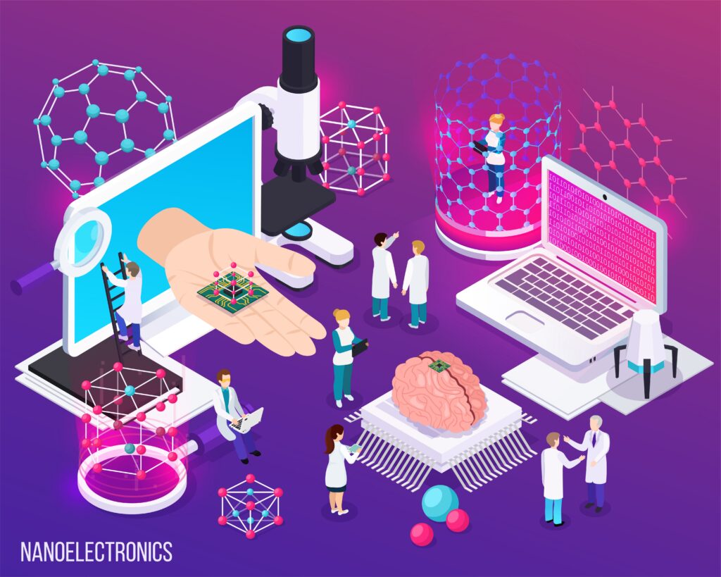
What are graphene-based semiconductors?
A graphene-based semiconductor is an electronic device that uses graphene as the primary conductive material instead of silicon. Graphene’s atomic structure allows electrons to move extremely quickly, which can improve chip performance and energy efficiency.
Why Graphene Is Unique
Graphene offers several remarkable physical properties that make it attractive for semiconductor applications:
- Extremely high electron mobility compared to silicon
- Exceptional thermal conductivity, allowing efficient heat dissipation
- Mechanical flexibility, enabling flexible electronics
- Atomic-scale thickness, which supports miniaturized devices
Because of these characteristics, graphene has the potential to improve the speed and efficiency of semiconductor chips used in high-performance computing.
However, graphene also presents a key challenge. Unlike silicon, it does not naturally have a bandgap, which is necessary for turning electronic signals on and off. Researchers are actively working on techniques such as bandgap engineering, graphene nanoribbons, and heterostructures to solve this issue.
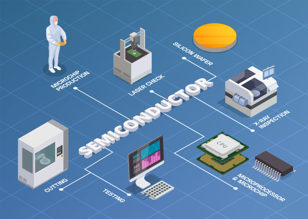
Why Silicon Semiconductors are Reaching Their Limits
Silicon has been the dominant material used in semiconductor manufacturing for over 50 years. Its electrical properties and manufacturing scalability made it the ideal foundation for modern electronics.
However, several challenges are emerging as silicon technology approaches its limits.
Scaling Limitations
When transistor sizes shrink below about 5 nanometers, leakage currents increase and chip performance declines.
Thermal Management Issues
Modern processors contain billions of transistors packed closely together, which leads to significant heat generation.
Rising Fabrication Costs
Producing advanced semiconductor chips requires highly complex manufacturing processes such as extreme ultraviolet lithography, making production increasingly expensive.
These challenges are motivating researchers to investigate next-generation semiconductor materials, including graphene.
Graphene vs Silicon Semiconductors: Key Differences
Understanding the differences between graphene and silicon helps explain why graphene is attracting so much interest in the semiconductor industry.
| Property | Graphene-Based Semiconductors | Silicon Semiconductors |
| Electron mobility | Extremely high | Moderate |
| Heat conductivity | Very high | Lower |
| Mechanical flexibility | Flexible | Rigid |
| Manufacturing maturity | Emerging technology | Established industry |
| Device thickness | Atom-thin | Several nanometers |
Graphene offers superior electrical and thermal performance, but silicon still has the advantage of a mature manufacturing ecosystem. Because of this, many experts believe that future semiconductor devices will combine silicon and graphene technologies rather than replacing silicon completely.
How Semiconductors Drive the Digital Transformation
Today’s innovations – Artificial Intelligence (AI), Machine Learning (ML), 6G communications, IoT, and autonomous systems – require semiconductors that are
- Faster to process vast datasets in milliseconds
- Energy-efficient for longer battery life and sustainability
- Smaller to fit into compact devices
- Reliable and scalable for global production demands
Semiconductors make all this possible. Yet, silicon alone cannot handle the growing demand for speed and energy efficiency, leading industries to explore graphene as the next-generation semiconductor material.
Breakthrough Innovations in Graphene Semiconductor Technology
Although graphene research is still evolving, several innovations are pushing the technology closer to commercial adoption.
Graphene Field-Effect Transistors (GFETs)
GFETs are transistors that use graphene as the conductive channel between electrodes. These devices can operate at extremely high frequencies, making them promising for terahertz communication systems and advanced sensors.
Advanced Semiconductor Fabrication Techniques
Scientists are developing new fabrication methods that allow graphene to be integrated into semiconductor manufacturing processes. Techniques such as atomic layer deposition help create ultra-thin material layers necessary for nanoscale devices.
Hybrid Semiconductor Architectures
Many chip designers believe the future lies in hybrid semiconductor systems, where graphene layers work alongside silicon components. In these designs, graphene can improve heat management and signal transmission while silicon performs traditional logic operations.
Gurtej Singh Sandhu’s Semiconductor Process Breakthroughs (Micron Technology)
With 1,300+ U.S. patents, Sandhu is one of the world’s most prolific inventors in semiconductor fabrication. His patents cover technologies that make graphene and next-generation materials integration feasible:
- Atomic Layer Deposition (ALD): Enables ultra-thin, uniform layers for nanoscale transistors — a method now used in SSDs, smartphones, and AI chips.
- Oxygen-Free Titanium Coating: Improves chip stability, reducing oxidation and extending device lifespan.
- Pitch Doubling Technology: Increases memory density without enlarging chip size, enabling compact yet powerful devices.
These innovations laid the foundation for modern memory and will support graphene integration in future device architectures.
Applications of Graphene-Based Semiconductors
Graphene technology could transform multiple industries that rely on high-performance semiconductor devices.
Artificial Intelligence and Data Processing
AI systems require powerful processors capable of handling massive datasets quickly. Graphene-based semiconductors could improve the speed and efficiency of AI accelerators.
Next-Generation Wireless Communication
Future 6G communication networks will operate at extremely high frequencies. Graphene antennas and transistors can support these terahertz communication systems.
Flexible and Wearable Electronics
Graphene’s flexibility enables new device designs such as foldable displays, smart clothing, and wearable medical sensors.
Advanced Sensors and Medical Devices
Graphene transistors are highly sensitive to environmental changes, making them useful for biosensors and diagnostic technologies.
Benefits of Using Graphene-Based Semiconductors
- Speed & Efficiency: Graphene transistors can switch faster than silicon, enabling real-time AI and 6G performance.
- Thermal Control: Exceptional heat conductivity prevents overheating, increasing chip reliability.
- Miniaturization: Enables ultra-thin, flexible devices without compromising power.
- Sustainability: Reduces energy usage and supports greener fabrication.
- Future Integration: Compatible with hybrid silicon–graphene systems for gradual industry transition.
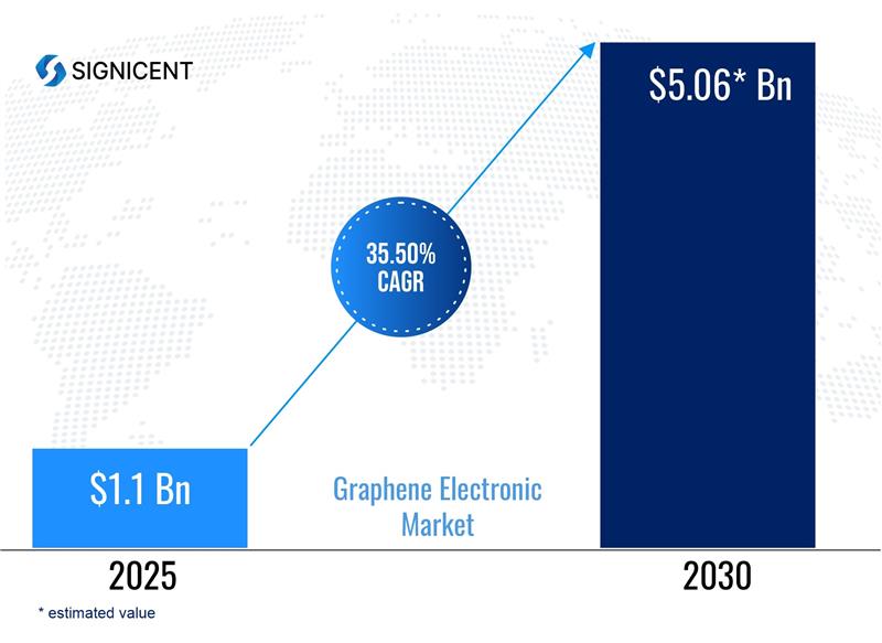
Market Outlook for Graphene-Based Semiconductors
The global semiconductor industry is actively exploring graphene technologies. As demand for faster and more energy-efficient electronics increases, graphene-based semiconductor solutions are attracting investment from both research institutions and major technology companies.
As per Signicent’s Market Research, the global graphene-based semiconductor market is projected to grow significantly over the next decade, driven by increasing demand for high-performance computing, advanced communication technologies, and energy-efficient electronic devices.
Key Players and Startups
Several organizations are already developing graphene electronics, including:
- Paragraf – graphene sensors and electronic devices
- Graphenea – graphene wafer manufacturing
- Vorbeck Materials – graphene conductive materials
- IBM and Samsung – research in advanced semiconductor materials
Market analysts expect the graphene semiconductor market to grow rapidly over the next decade as fabrication techniques mature and commercial products emerge.

Market analysts expect the graphene semiconductor market to grow rapidly over the next decade as fabrication techniques mature and commercial products emerge.
How Signicent Supports Semiconductor Innovation
Companies exploring graphene-based semiconductors must navigate complex technology landscapes, intellectual property challenges, and emerging market opportunities. Signicent helps organizations gain strategic insights to accelerate innovation in semiconductors and advanced materials.
Through patent landscape analysis, technology scouting, competitive benchmarking, market research, and partner identification, Signicent enables businesses to make informed decisions and stay ahead in the rapidly evolving semiconductor ecosystem.
Conclusion: The Future of Semiconductors Beyond Silicon
The semiconductor industry is entering a new era. As silicon technology approaches its limits, researchers are exploring innovative materials that can sustain the growth of computing performance.
Graphene-based semiconductors offer a compelling vision for the future of nanoelectronics. Their exceptional electrical conductivity, thermal performance, and structural flexibility could enable breakthroughs in artificial intelligence, high-speed communication, and advanced sensor technologies.
While silicon will continue to play a crucial role, graphene may become a powerful complementary material that extends the capabilities of modern semiconductor devices. As research advances and manufacturing methods improve, graphene could help shape the next generation of electronics — bringing faster, smarter, and more sustainable semiconductor technologies to the world.
FAQ’s About Graphene-Based Semiconductors
1. What are graphene-based semiconductors?
Graphene-based semiconductors are electronic devices that use graphene, a single layer of carbon atoms, as the conductive material instead of traditional silicon. Graphene allows electrons to move much faster, which can improve chip speed, energy efficiency, and heat management in advanced semiconductor technologies.
2. Can graphene replace silicon in semiconductor chips?
Graphene is unlikely to completely replace silicon in the near future. Silicon has a well-established manufacturing ecosystem, while graphene technology is still developing. Most experts believe future chips will use hybrid semiconductor architectures, combining silicon logic with graphene interconnects or transistors for improved performance.
3. Why is graphene considered important for next-generation semiconductors?
Graphene is important because it offers extremely high electron mobility, excellent thermal conductivity, and atomic-scale thickness. These properties make it attractive for applications such as AI processors, 6G communication systems, high-frequency electronics, and flexible devices.
4. What are the biggest challenges in developing graphene-based semiconductors?
The biggest challenge is that graphene does not naturally have a bandgap, which is required for switching electronic signals on and off. Researchers are exploring solutions such as graphene nanoribbons, chemical doping, and graphene heterostructures to enable reliable semiconductor behavior.
5. Which industries could benefit from graphene semiconductor technology?
Several industries could benefit from graphene-based semiconductors, including artificial intelligence computing, telecommunications, wearable electronics, automotive sensors, and medical diagnostics. These sectors require faster, smaller, and more energy-efficient semiconductor devices.